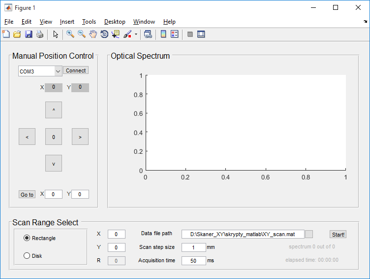
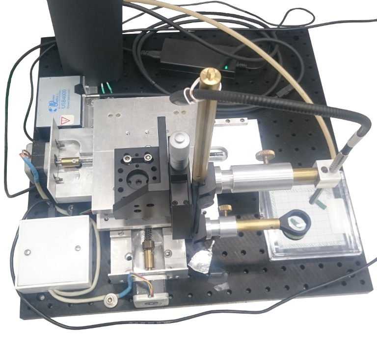
This page illustrates a very useful setup that I designed and build at the begining of my PhD studies. It is a computer-controlled reflectivity mapping setup, allowing for mapping of an entire 3-inch wafer.
A XY mapping setup
Some of the samples that we use in the lab are higroscopic - they require extra care and should not be exposed to air for an extended period of time. In such cases it's a good idea to include a box, where a sample is kept during mapping, with a constant flow of nitrogen. You can see an example of such a box below.
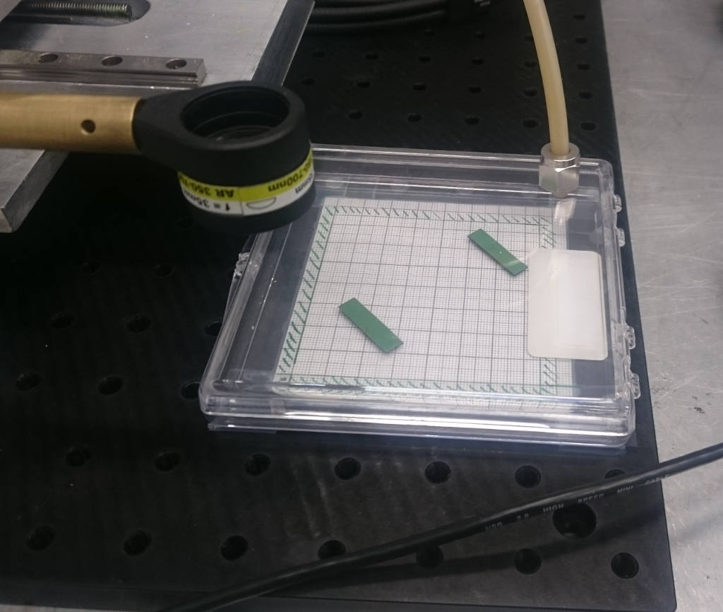
A box with a constant flow of nitrogen.
Why is this setup useful?
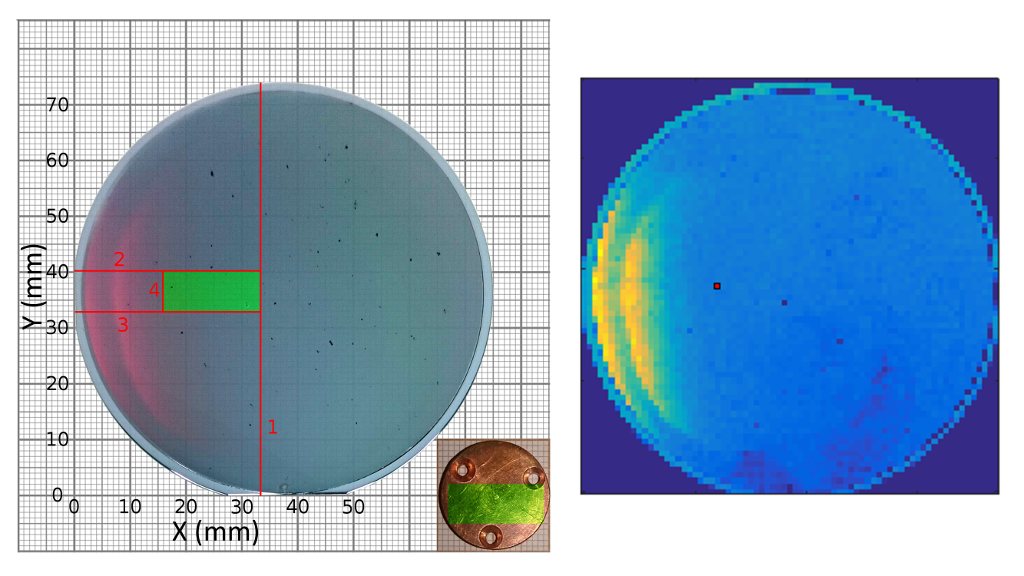
In my studies the samples were grown with a gradient of thickness. This means that their properties depend on the place on the sample. Sometimes only a very narrow path on the sample exhibits interesting properties. Its important to be able to find that areas of the sample.
Below you can see a 3-inch wafer with an interesting area indicated in green. Red lines indicate consecutive cuts of the wafer, to get to the interesting region. In the right lower part of that picture you can see
a typical sample holder, that we glue our samples to, to perform low temperature measurements. As you can see, the wafers area is huge compared to the holder size. The promising area, indicated in green, was selected based on a reflectivity measurement, performed with a 1 mm step, shown to the right. The image to the right shows reflectivity intensity (blue - low, yellow - high), for a given wavelength.
Example of xy mapping application