|



Two-dimensional crystals with a honeycomb structure, including the famous graphene, have already revolutionized nanoscience and have the potential to revolutionize common technologies, as well. Therefore, it is highly desirable to develop industrial-scale methods for their production. However, despite substantial investments in the development of growth techniques for atomically thin crystals, the best quality monolayers are currently still obtained using exfoliation, i.e. due to the mechanical detachment of individual atomic layers from the bulk crystal. For example, small graphene flakes exfoliated from bulk graphite exhibit superior electrical properties when compared to graphene grown on large substrates.
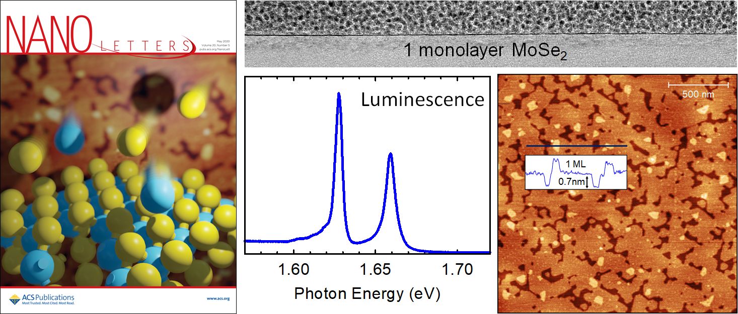
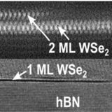
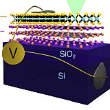
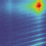
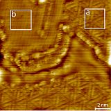
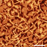
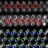
Similarly, optical properties of two-dimensional transition metal dichalcogenides (TMDs, e.g. molybdenum diselenide, MoSe2) long time have been fully revealed only for layers mechanically placed between layers of hexagonal boron nitride (hBN). Below, there are figures showing how we approach this problem by MBE growth of MoSe2 (Fig. 1a) and WSe2 (Fig. 1b) directly on exfoliated hBN.

Fig. 1a. Nano Letters, where we report on first MBE grown MoSe2 monolayer with well resolved excitonic transitions on photoluminescence spectrum. Both cross-section and AFM image reveal that most of area is covered by monolayer, with only small grains of bilayers. Importantly, no mechanical postprocessing was performed after growth.
 |
"Narrow excitonic lines and large-scale homogeneity of transition metal dichalcogenide monolayer grown by molecular beam epitaxy on hexagonal boron nitride",
W. Pacuski, M. Grzeszczyk, K. Nogajewski, A. Bogucki, K. Oreszczuk, J. Kucharek, K.E. Połczyńska, B. Seredyński, A. Rodek, R. Bożek, T. Taniguchi, K. Watanabe, S. Kret, J. Sadowski, T. Kazimierczuk, M. Potemski, P. Kossacki,
Nano Letters 20, 3058 (2020).


 ,
Press release EN, PL. ,
Press release EN, PL.
|

Fig. 1b. Nano Letters, where we report on first WSe2 monolayer grown by MBE on hBN. In this work we used exfoliated hBN.
 |
"WSe2 Monolayers Grown by Molecular Beam Epitaxy on hBN",
J. Kucharek, M. Raczynski, R. Bozek, A. Kaleta, B. Kurowska, M. Bilska, S. Kret, T. Taniguchi, K. Watanabe, P. Kossacki, M. Goryca, W. Pacuski,
Nano Letters 25, 17275 (2025).


|
 |
"Magnetic field induced polarization enhancement in the photoluminescence of MBE-grown WSe2 layers",
M. C. Kuna, M. Raczyński, J. Kucharek, T. Taniguchi, K. Watanabe, T. Kazimierczuk, W. Pacuski, P. Kossacki,
Solid State
Commun. 409, 116263 (2026).

|
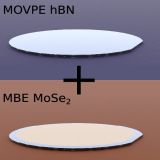
Moreover, thanks to cooperation with MOVPE lab, we obtained really large ares of good optical quality MoSe2 monolayer by direct MBE growth on epitaxial (MOVPE) hBN, on whole 2" wafer. Below, there is a scheme of our growth.

Fig. 2a. Combining MOVPE growth of hBN and MBE growth of MoSe2 we are able to obtain 2" wafers with good optical quality TMD monolayers.

Fig. 2b. Two inch large wafer with MoSe2 monolayer grown on hBN
 |
"Heteroepitaxial growth of high optical quality, wafer-scale van der Waals heterostrucutres",
K. Ludwiczak, A. K. Dąbrowska, J. Binder, M. Tokarczyk, J. Iwański, B. Kurowska, J. Turczyński, G. Kowalski, R. Bożek, R. Stępniewski, W. Pacuski, A.Wysmołek,
ACS Appl. Mater. Interfaces 13, 47904 (2021).


|
 |
"Large-Area Growth of High-Optical-Quality MoSe2/hBN Heterostructures with Tunable Charge Carrier Concentration",
K. Ludwiczak, A. K. Da?browska, J. Kucharek, J. Rogoża, M. Tokarczyk, R. Bożek, M. Gryglas-Borysiewicz, T. Taniguchi, K. Watanabe, J. Binder, W. Pacuski, A. Wysmołek,,
ACS Appl. Mater. Interfaces 16, 49701(2024).


|
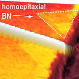
Moreover, MOCVD BN can be also improved by homoepitaxial growth on exfoliated hBN,
 |
"Homoepitaxy of Boron Nitride on exfoliated hexagonal Boron Nitride flakes",
J. Binder, A. K. Dabrowska, M. Tokarczyk, A. Rousseau, P. Valvin, R. Bozek, K. Nogajewski, G. Kowalski, W. Pacuski, B. Gil, G. Cassabois, R. Stepniewski, A. Wysmolek,
Nano Letters 24, 6990 (2024).


|
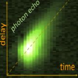
Further papers on TMDs include Four Wave Mixing spectroscopy performed on MoSe2 MBE grown on exfoliated hBN,
 |
"Coherent imaging and dynamics of excitons in MoSe2 monolayers epitaxially grown on hexagonal boron nitride",
K. E. Połczyńska, S. Le Denmat, T. Taniguchi, K. Watanabe, M. Potemski, P. Kossacki, W. Pacuski, J. Kasprzak,
Nanoscale 15, 6941 (2023).
 , ,

|
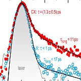
precise measurements of ultrashort exciton lifetime,
 |
"Short excitonic lifetimes of MoSe2 monolayers grown by molecular beam epitaxy on the hexagonal boron nitride",
K. Oreszczuk, W. Pacuski, A. J. Rodek, M. Raczynski, T. Kazimierczuk, K. Nogajewski, T. Taniguchi, K. Watanabe, M. Potemski, Piotr Kossacki,
2D Materials 11, 025029 (2024).
|
and Raman scattering excitation performed on both exfoliated and MBE MoSe2 on hBN,
 |
"Raman scattering excitation in monolayers of semiconducting transition metal dichalcogenides",
M. Zinkiewicz, M. Grzeszczyk, T. Kazimierczuk, M. Bartos, K. Nogajewski, W. Pacuski, K. Watanabe, T. Taniguchi, A. Wysmołek, P. Kossacki, M. Potemski, A. Babiński, M. R. Molas,
npj 2D Materials and Applications 8, 2 (2024) .


|
growth of (Mo,Mn)Se2 on various substrates,
growth of MoTe2 on exfoliated hBN,
and finally, growth and transport studies of MoTe2 bilayer on GaAs (111),
 |
"Charge Transport in MBE-grown 2H-MoTe2 Bilayers with Enhanced Stability Provided by AlOx Capping Layer",
Z. Ogorzałek, B. Seredyński, S. Kret, A. Kwiatkowski, K. P. Korona, M. Grzeszczyk, J. Mierzejewski, D. Wasik, W. Pacuski, J. Sadowski and M. Borysiewicz,
Nanoscale 12, 16535 (2020).
|
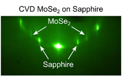
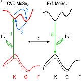
MBE is useful also for electron diffraction study of materials grown by CVD method (which is not performed in UHV, therfore not equipped with RHEED):

 |
"Twisted MoSe2 Homobilayer Behaving as a Heterobilayer ",
A. Karmakar, A. Al-Mahboob, N. Zawadzka, M. Raczyński, W. Yang, M. Arfaoui, Gayatri, J. Kucharek, J. T. Sadowski, H. Suk Shin, A. Babiński, W. Pacuski, T. Kazimierczuk, M. R Molas,
Nano Letters 24, 9459 (2024).


|
|
